An authoritative analysis of B2B micro-electronics architectures, high-density PCBs, and structural engineering paradigms driving the global edge-computing and wearable technology sectors.
Next-generation wearable devices—ranging from medical-grade biometric monitors to industrial AR smart glasses—require high-density interconnect (HDI) PCBs and ultra-compact memory layouts that balance structural stability with thermal efficiency.
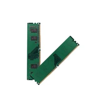
Latency-sensitive wearable data networks require edge preprocessing. By integrating low-latency, high-frequency DDR4 and DDR5 memory modules directly at the hardware layer, field devices can support real-time local machine learning models without heavy cloud dependency.
Unlike standard desktop components, wearable-grade hardware elements face severe physical challenges, including temperature fluctuation, continuous humidity, and kinetic impact, requiring 100% stress-tested structural backbones.
Global procurement agents face unprecedented bottlenecks when sourcing semiconductor substrates, custom-sized high-frequency PCBs, and ruggedized memory architectures. In critical sectors like aerospace, industrial automation, and telemetry-tracking, hardware failure translates to systemic shutdown.
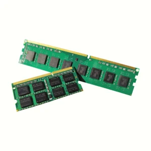
B2B buyers seek manufacturing partners who offer comprehensive quality validation systems—specifically, automated optical inspection (AOI), in-circuit testing (ICT), and system-level thermal validation under continuous loading. Furthermore, securing stable DRAM chips through long-term supply chain partnerships is vital to maintaining predictable production cadences and insulating against global wafer shortages.
Vorynex Memory Technology (China) Co., Ltd. addresses these systemic vulnerabilities by serving as a dedicated OEM/ODM manufacturing node, combining agile production facilities with an expansive semiconductor supply chain of over 1,200 partners.
How high-frequency substrates, custom thermal management, and advanced RAM modules form the bedrock of complex smart ecosystems.
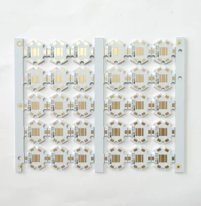
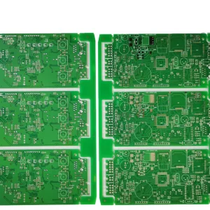
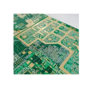
Medical tracking devices, high-end smartwatches, and rugged location beacons require micro-scale substrates. Utilizing advanced high-frequency multi-layer boards ensures trace integrity, reducing electromagnetic interference (EMI) across Bluetooth, Wi-Fi, and 5G cellular bands.
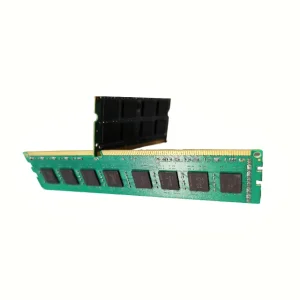
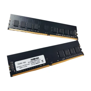
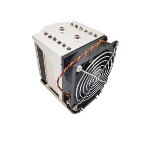
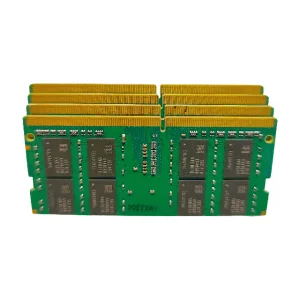
Wearable systems rely heavily on central on-premise hubs. Implementing high-density server configurations—such as DDR4 ECC Server Memory Modules paired with specialized LGA4189-N96 Heat Sinks—ensures that incoming telemetry streams are processed with zero down-time or bit-flip errors.
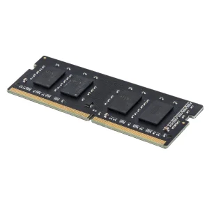
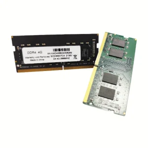
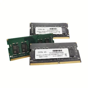
AR systems processing high-bandwidth 3D environmental mapping require ultra-high data rates. The inclusion of low-latency SO-DIMM and customized DDR4/DDR5 system memory modules prevents visual stuttering, lowering user fatigue and ensuring reliable operation in hazardous environments.
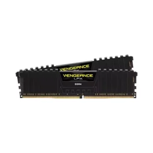
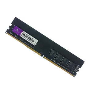
As wearable data processing pipelines expand, traditional DDR3 and base DDR4 modules are being replaced by DDR5 architectures. DDR5 introduces on-die ECC (Error Correction Code) and dual 32-bit subchannels, which significantly boost read-write throughput for complex edge servers and processing modules.
On the substrate level, high-frequency materials such as Rogers 4000 Mixed Pressure and High-TG170 FR4 boards are becoming critical. These materials allow micro-electronic systems to run at speeds over 10 GHz with minimal signal degradation and dielectric loss, which is essential for Wearable AI and spatial computing designs.
In addition, miniaturized components need efficient heat dissipation. Specialized aluminum PCBs and advanced copper heat-pipe assemblies are designed to draw heat away from the CPU and RAM. This ensures that compact wearable housings do not overheat, maintaining system stability during continuous use.
A deep insight into our industrial footprint, capacity scale, and scientific development guidelines.
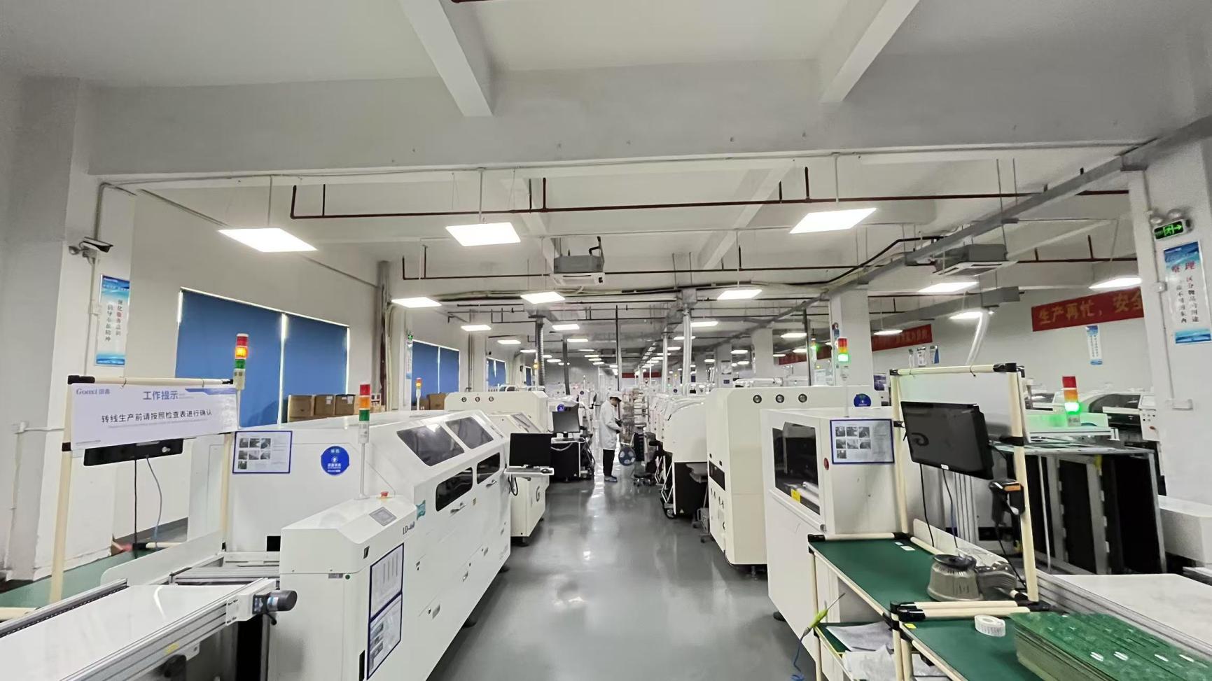
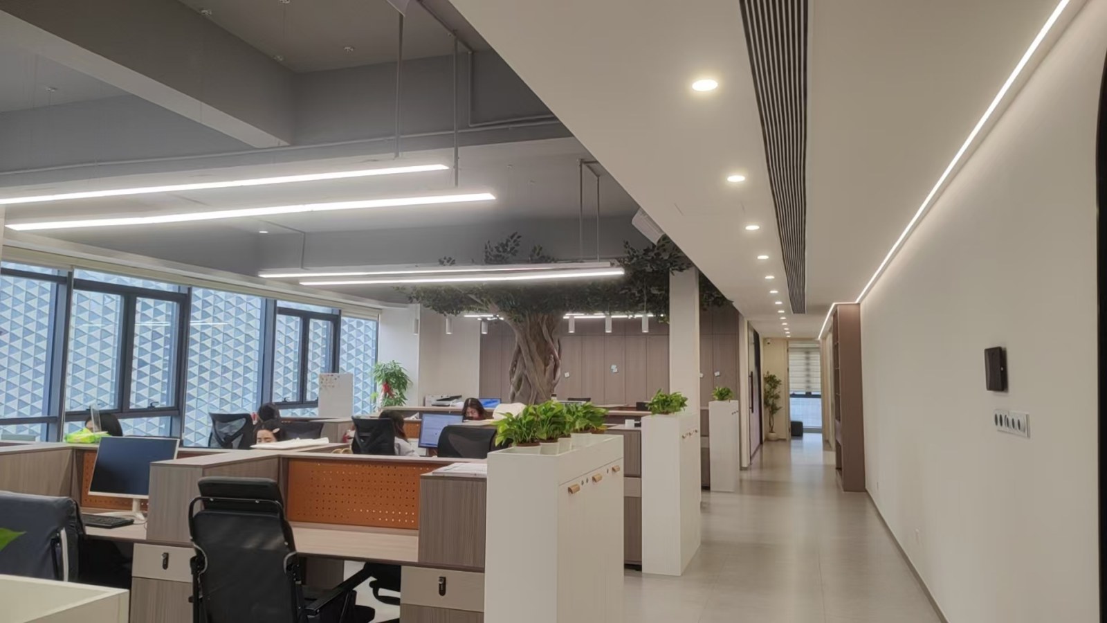
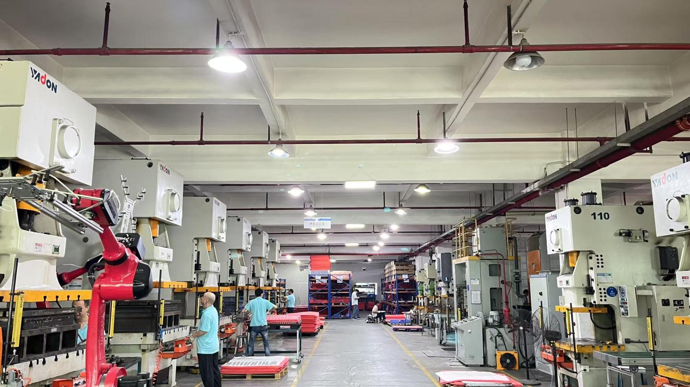
Founded in 2016, our modern facility spans approximately 320㎡. We specialize in precision engineering and high-frequency wave-soldering processes, allowing us to maintain tight component clearances and produce durable, high-performance electronics.
Our research and development team of approximately 180 R&D engineers focuses on frequency optimization, custom PCB layouts, and thermal management. We launched around 240 new product models in the past year, covering DDR4, DDR5, and specialized industrial memory solutions.
With an annual export revenue of USD 12 million and over 12 years of industry experience, we serve customers across North America, Europe, Southeast Asia, the Middle East, and South America. We collaborate with over 1,200 supply chain partners to ensure a stable supply of DRAM chips.

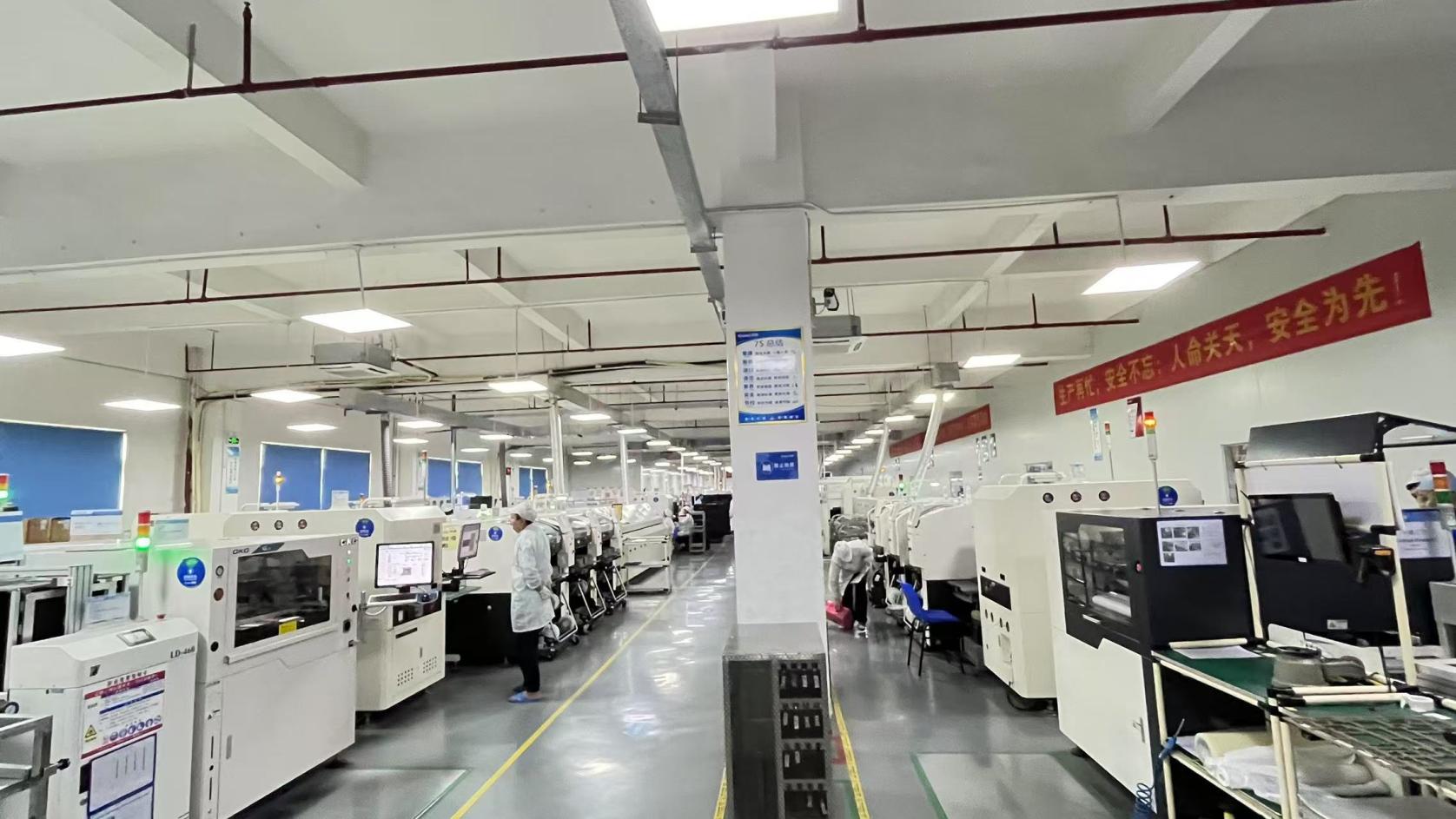
Quality control at Vorynex is managed by a team of 45 professional QC staff. Every manufacturing run undergoes a multi-phase inspection process to ensure reliability and performance in demanding environments:
We use lead-free HASL processes, high-TG FR4, and Rogers materials. Our products meet RoHS, CE, and FCC standards, ensuring they comply with environmental and regulatory requirements in North American and European markets.
DRAM Sorting: Only original major-brand die wafers (Samsung, SK Hynix, Micron) are selected for critical systems.
PCB Thickness Tolerance: Controlled within ±0.05mm across all multi-layer and high-frequency runs.
Impedance Match: Configured precisely at 50Ω and 100Ω differential structures for clean data signals.
Answers to common B2B engineering and purchasing questions about wearable components, memory modules, and high-frequency boards.