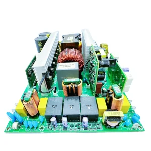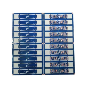
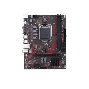
In the rapidly changing world of electronics manufacturing, multi-layer printed circuit boards (PCBs) are the core foundation of modern computing power, telecommunications, and industrial automation systems. As global industries demand higher frequency operations, faster signal speeds, and smaller footprints, multi-layer PCBs with advanced stack-ups, microvias, and low-loss substrates have become essential.
Currently, the global multi-layer circuit board industry is undergoing a major shift. The transition toward high-performance computing (HPC), AI-driven server architectures, and automotive electrification has pushed design requirements past traditional boundaries. Simple, rigid double-sided boards are no longer sufficient. Today's commercial needs require multi-layer stack-ups that scale from 4 to over 32 layers. These layouts are designed to support complex trace routing, minimize electromagnetic interference (EMI), and manage strict power and thermal conditions.
By using controlled impedance models, designers can maintain signal integrity over long distances and at higher frequencies. Choosing the right raw materials—such as high-Tg (glass transition temperature) FR-4, polytetrafluoroethylene (PTFE), and polyimide—determines how well the board performs under thermal stress and environmental challenges. Understanding these material characteristics helps manufacturers build reliable systems that withstand the thermal cycles common in high-density installations.
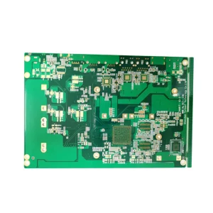
Utilizing blind, buried, and micro-via technologies to build highly complex connections within minimal physical footprints, optimizing board density and signal paths.
Precise impedance calculations and robust layer stack-up configurations reduce crosstalk, signal degradation, and power loss in high-frequency applications.
Balanced component layouts and efficient routing strategies lower manufacturing costs while maintaining high electrical and thermal performance.
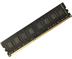
The performance of a multi-layer circuit board depends heavily on the materials used. Designers must balance electrical behavior, thermal limits, and physical durability. Factors like the Dielectric Constant (Dk) and Dissipation Factor (Df) are critical when selecting copper-clad laminates (CCL). Lower values of Dk and Df reduce propagation delays and signal loss, which is essential for high-frequency applications like DDR5 memory routing, 5G communications, and server motherboards.
Vorynex Memory Technology focuses on advanced materials and precise stack-up engineering. Modern PCB layouts require balanced layering to prevent warping during lead-free reflow soldering, where temperatures can exceed 260°C. By placing prepreg and core materials symmetrically, internal stresses are minimized. High-Tg materials (Tg > 170°C) help ensure the board remains stable under long-term thermal loads.
Additionally, adding specialized thermal vias, thick copper cores, and thermal interface materials (TIMs) improves heat dissipation. This prevents localized hotspots that could cause premature component failure, ensuring consistent performance.
From high-speed computing modules to rugged industrial equipment, multi-layer PCBs provide the foundational reliability required across diverse environments and applications.
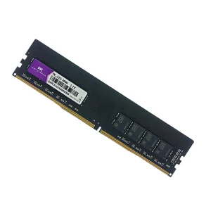
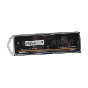
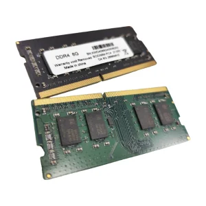
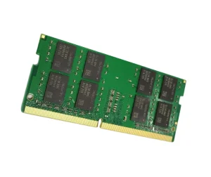
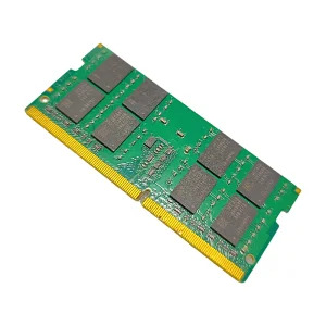
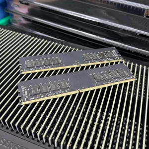
Supports complex, multi-channel memory layouts like DDR4 and DDR5 RAM. Strict impedance control is essential to handle high data rates, preventing data loss and ensuring continuous server operation.
High-voltage and high-current power stages require thick copper layers (up to 4oz or more) to support solar inverters and battery management systems, ensuring efficiency and safety.
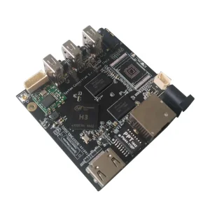
Compact IoT devices rely on HDI PCBs with blind and buried vias to fit Wi-Fi modules, sensors, and power systems into tiny footprints, maintaining performance without compromising space.
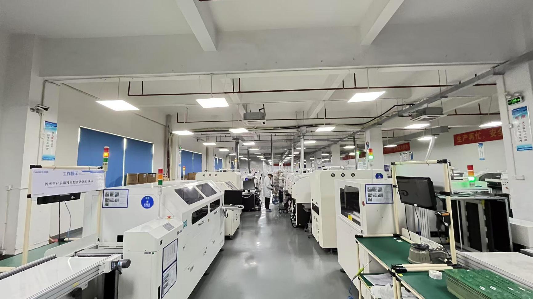
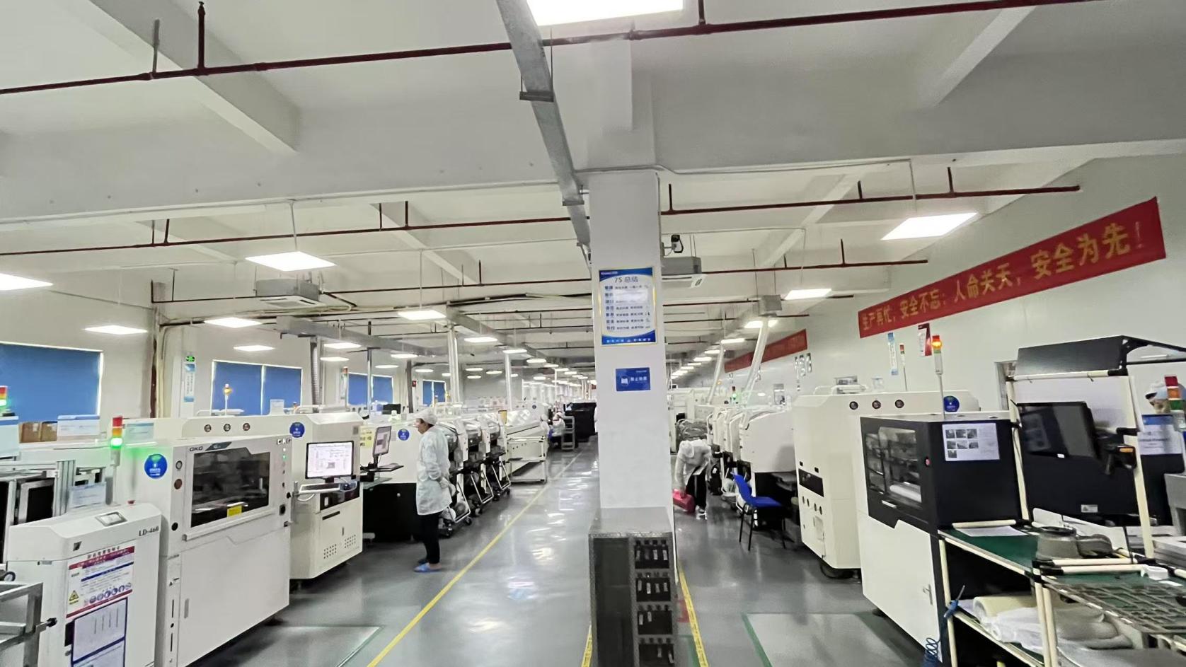
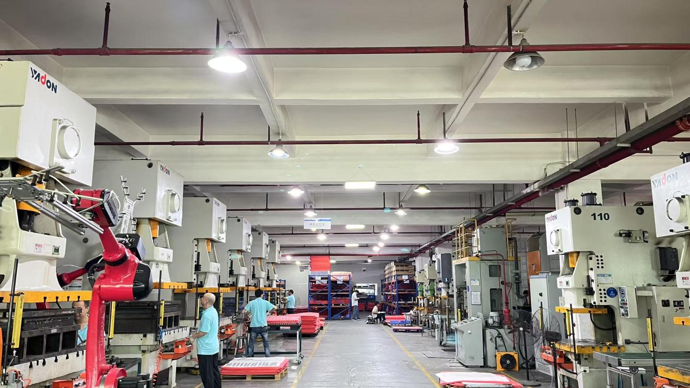
Vorynex Memory Technology (China) Co., Ltd. is a professional DDR5 memory manufacturer and OEM/ODM solution provider specializing in high-performance memory modules for global markets. Established in 2016, the company has developed strong manufacturing and engineering capabilities over the years. With a modern production facility covering approximately 320㎡, Vorynex focuses on delivering stable, high-speed, and energy-efficient memory solutions for gaming, industrial, and enterprise applications.
Vorynex has achieved an annual export revenue of approximately USD 12 million, supported by 6 years of export experience and over 12 years of industry experience in memory and semiconductor-related fields. With a strong international trade background, the company serves key markets including North America, Europe, Southeast Asia, the Middle East, and South America. Vorynex collaborates with more than 1,200 supply chain partners, enabling stable sourcing of high-quality DRAM chips and components.
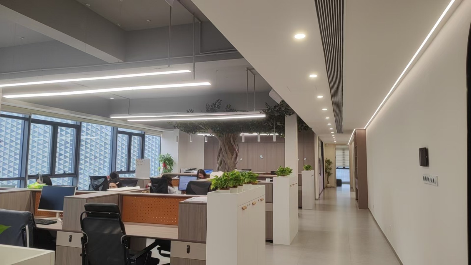
Its primary customer base includes brand distributors, system integrators, industrial equipment manufacturers, and gaming hardware companies. Vorynex also has strong R&D capabilities, supported by a team of approximately 180 R&D engineers, focusing on memory architecture optimization, compatibility enhancement, and thermal performance improvement. Customization is fully supported, including frequency tuning, PCB design customization, heat sink design, branding (private label), and firmware optimization. In the past year, the company successfully launched around 240 new product models, covering DDR4, DDR5, and specialized industrial memory solutions.
To ensure consistent product reliability, Vorynex maintains strict quality control standards, including 100% functional testing, aging tests, compatibility testing, and high-temperature stress testing. Product inspection methods include automated optical inspection (AOI), in-circuit testing (ICT), and final system-level validation. The quality assurance team consists of approximately 45 professional QC staff ensuring consistent quality.

As electronic systems become faster and more compact, the technology roadmap for multi-layer PCBs must evolve. Future designs are moving toward embedded components, where passive parts are placed directly into the internal layers. This shortens signal paths and frees up outer board space. Additionally, optical interconnects are emerging to replace copper traces, helping bypass traditional physical limits of data transfer.
Developing HDI techniques to support next-generation BGAs, lowering assembly risks and increasing wiring density.
Qualifying new fluorine-based and polyphenylene ether (PPE) resin systems to support the thermal demands of DDR5 and high-speed communications.
Adopting halogen-free materials and waste-reducing plating methods, aligning with RoHS and REACH regulations.