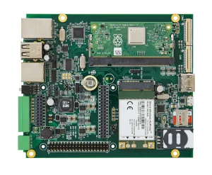
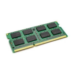
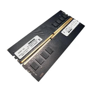
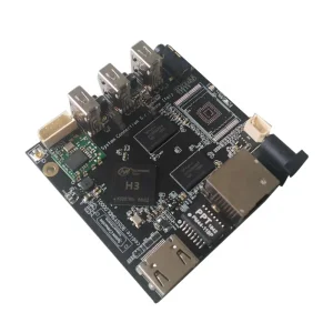
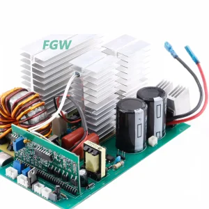
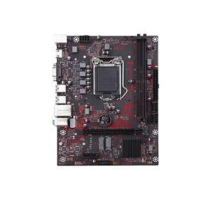
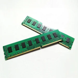
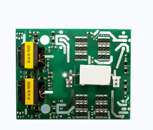
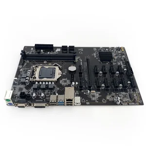
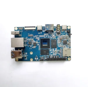
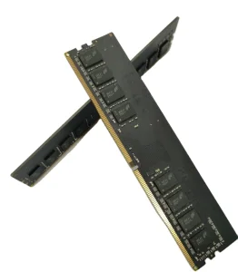
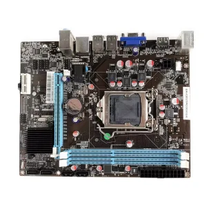
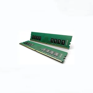
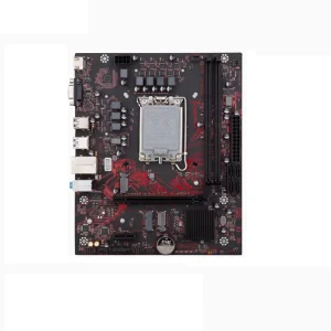
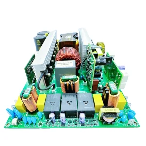
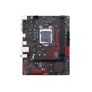
Explore our leading catalog of industrial motherboards, high-frequency PCBAs, and speed-optimized memory modules.
An authoritative breakdown of material sciences, structural designs, and manufacturing requirements reshaping the global high-speed PCB ecosystem.
The transition to sub-6GHz and mmWave bands demands PCBs with exceptionally low dielectric constant (Dk ≤ 3.0) and minimal dissipation factor (Df ≤ 0.0015). This minimizes transmission delay and prevents thermal breakdown in radio-frequency antennas.
Automotive safety systems operating at 77GHz and 79GHz require high-reliability hybrid stack-ups. Materials such as PTFE (Polytetrafluoroethylene) bonded with FR4 allow automotive OEMs to balance cost efficiency with thermal performance under extreme engine-compartment temperatures.
Next-generation cloud storage, optical transceivers, and AI processors run ultra-high data transfer protocols (PCIe Gen 5/6 and DDR5). They demand ultra-low loss (ULL) laminates to mitigate impedance mismatches, crosstalk, and skin-effect losses at ultra-high frequencies.
In high-frequency design, the choice of laminate material dictates the physical limits of signal transmission. Traditional FR4 substrates fail at frequencies exceeding 3 GHz due to excessive dielectric absorption and dispersion. To prevent critical signal degradation, our manufacturing facility leverages high-grade materials including Rogers (e.g., RO4003C, RO4350B), Taconic, Arlon, and Nelco.
These composite substrates guarantee stability across varying moisture levels and operating temperatures, keeping your signal path clear, minimizing transmission losses, and mitigating phase distortion in complex phase-array radar systems.
Addressing the strict parameters required by supply chain managers and hardware engineering leads during strategic sourcing.
Global procurement teams must secure components that adhere strictly to RoHS, REACH, and UL certifications. Furthermore, military and aerospace sectors require AS9100 and ISO 9001 certifications, backed by complete materials traceability reports.
Disruptions in specialized copper-clad laminates (CCL) can stall production lines. Partnering with a manufacturer integrated with over 1,200 raw material and chemical vendors guarantees continuous production even during global silicon or fiberglass shortages.
Procuring raw PCBs without rigorous Design for Manufacturing (DFM) analysis leads to low assembly yields. Suppliers must provide comprehensive front-end engineering reviews to adjust trace clearances, pad dimensions, and drilling tolerances before micro-drilling begins.
Our operational capabilities match international high-frequency design regulations.
| Parameter / Process | Standard Capabilities | Advanced Engineering Thresholds |
|---|---|---|
| Layer Count | 2 - 16 Layers | Up to 32 Layers (Hybrid Stack-ups) |
| Laminate Materials | FR4, High-Tg, Halogen-Free | Rogers, PTFE, Taconic, Nelco, Megtron 6 |
| Dielectric Constant (Dk) | 3.5 - 4.8 (±0.05) | 2.2 - 3.5 (±0.02) |
| Dissipation Factor (Df) | 0.015 - 0.025 | 0.001 - 0.005 |
| Impedance Control Tolerance | ±8% - ±10% | ≤ ±5% |
| Aspect Ratio (Max) | 8:1 | 12:1 |
| Min. Line Width / Spacing | 3 mil / 3 mil | 2 mil / 2 mil |
| Surface Finishes | HASL, Lead-Free HASL, OSP | ENIG, ENEPIG, Immersion Silver, Immersion Tin |
Vorynex Memory Technology (China) Co., Ltd. — Engineering Precision, High-Performance Semiconductor and High-Frequency Board Systems.
Established in 2016, Vorynex Memory Technology (China) Co., Ltd. has developed strong manufacturing and engineering capabilities over the years. Leveraging our deep expertise in high-speed data transmission and semiconductor memory configurations, we provide robust high-frequency board engineering, OEM/ODM production, and specialized PCBA services.
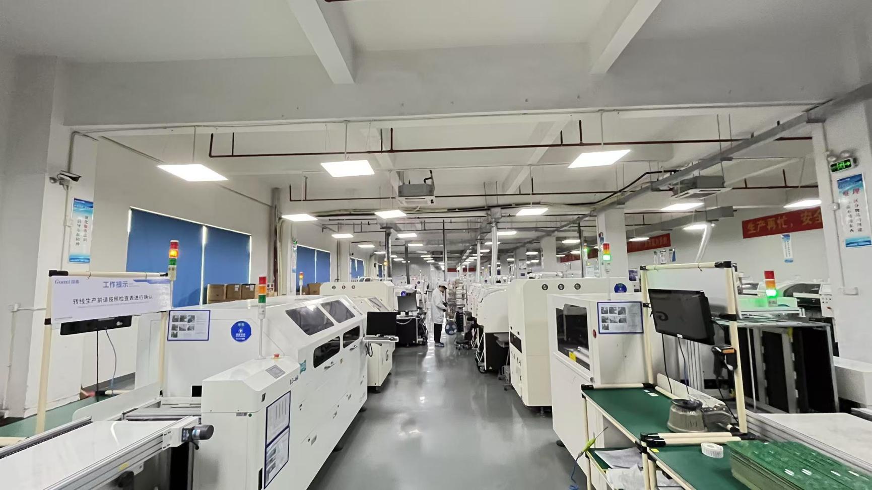
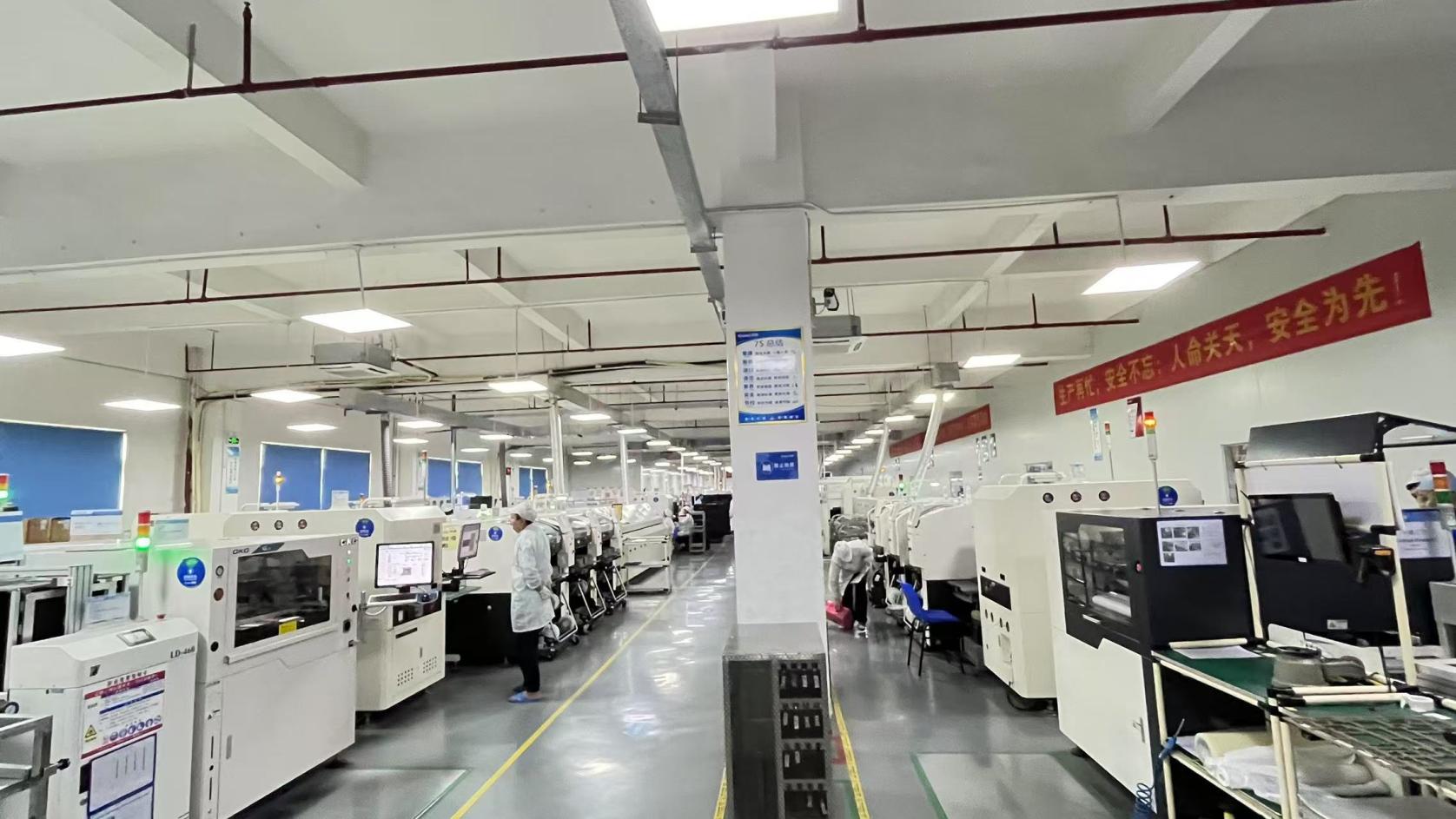
Reliability at high frequencies demands absolute quality. Our facility features advanced cleanroom spaces and applies rigorous inspection paradigms across all stages of production:
With our strong engineering team and state-of-the-art facility, we support full customization to meet the precise requirements of brand distributors, system integrators, and industrial manufacturers:
Translating material sciences into high-reliability systems for global markets.
Utilizing high-stability ceramics and PTFE composites to ensure microwave radars function flawlessly across extreme thermal and mechanical transitions.
High-layer count multi-layer PCBs and hybrid stack-ups engineered to minimize crosstalk in baseband processing units and high-speed remote radio heads.
Delivering low-loss motherboards designed for next-generation system architectures, supporting modern high-capacity DDR5 layouts and fast PCIe lanes.
An forward-looking projection of high-frequency PCB development, material changes, and alignment with next-generation processing standards.
By 2026, the electronics industry will transition toward next-generation ultra-low loss (ULL) laminates. This shift is driven by the rise of PCIe Gen 6 and high-speed data transmission systems. The focus will center on hydrocarbon and modified polyimide (MPI) substrates that maintain signal integrity at frequencies exceeding 100 GHz.
Our facility is adapting by incorporating ultra-smooth HVLP (Hyper Very Low Profile) copper foils, reducing the average conductor roughness to less than 1.0 μm. This helps counter current crowding (skin effect) at higher frequencies.
As system boards shrink, the demand for Any-Layer HDI (High-Density Interconnect) and microvia structures is increasing. Embedded passive components (resistors and capacitors) within inner layers help free up surface space and minimize parasitic inductance.
Vorynex is actively updating its microvia drilling techniques. Using advanced UV-CO2 hybrid laser drills, we can execute via drilling down to 2.5 mil (63.5 μm), ensuring reliable alignment and solid connectivity across high-layer boards.
Bridging Chinese manufacturing speed with global service standards and regulatory compliance.
Our technical team provides on-demand remote DFM advice, assisting with layout changes and stack-up verification in real-time across key global timezones.
We supply complete compliance documentation with each batch, including RoHS reports, REACH declarations, and UL flame-retardant performance ratings.
By leveraging customs clearances and strategic warehouse points in Southeast Asia and Europe, we keep logistics smooth and transit times short.
In-depth responses to essential manufacturing and material questions, helping you streamline your sourcing process.
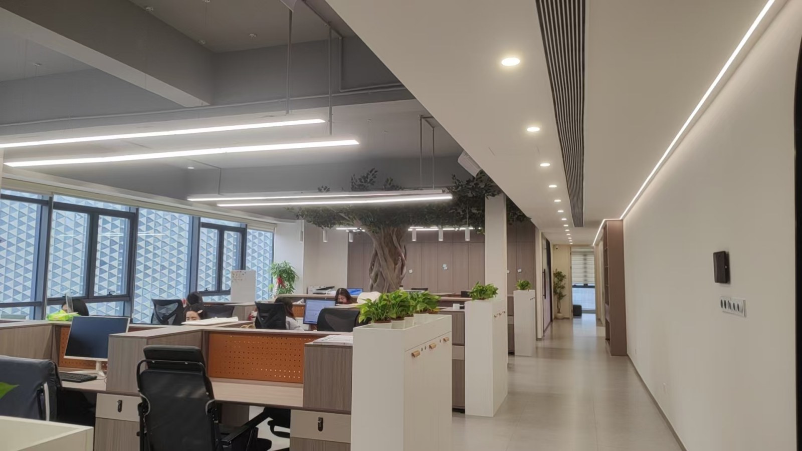
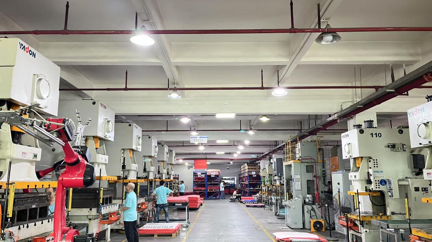
A look inside our advanced manufacturing, assembly, and quality control departments.

Our complete range of industrial PCBA, ODM development boards, and memory configurations.