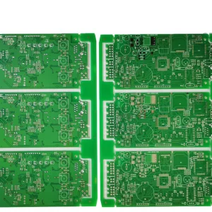
In modern electrical engineering, thermal dissipation and current-carrying capacity are the twin pillars of design stability. Standard printed circuit boards with typical 1oz copper (35µm) are increasingly inadequate for handling high electrical currents. This is where Thick Copper Circuit Boards (also known as heavy copper PCBs, typically utilizing 3oz to 20oz copper or 105µm to 700µm) step in.
By increasing the copper thickness of outer and inner layers, we significantly expand the cross-sectional area of the PCB's conductive pathways. This modification dramatically reduces electrical resistance, mitigates thermal buildup, and strengthens mechanical durability at contact points. The engineering threshold for thick copper fabrication requires specialized etching techniques, customized plating regimes, and highly compatible thermal interfaces (such as copper-aluminum composite structures) to prevent trace undercut and maintain substrate integrity.
As high-performance systems demand higher wattages in tighter spaces, thick copper technology has evolved from a niche industrial choice to an essential baseline for enterprise-grade power distribution networks (PDNs), EV charging hardware, and smart-grid controllers.
Our heavy copper boards are manufactured using advanced chemical plating processes, offering extreme heat conduction properties and low impedance.
How our thick copper substrate optimization changes the performance landscape for high-stress system architectures.
By replacing standard FR4 traces with heavy copper tracks, the PCB acts as its own heatsink, directing thermal energy away from critical active components such as MOSFETs, processors, and high-frequency memory modules.
Allows high currents to pass through narrow traces without suffering trace burnout or critical system resistance spikes. Essential for automotive EV powertrains and dual-channel high-density power grids.
Heavy copper plating enhances mechanical strength at connector pins, mounting holes, and solder points, preventing substrate cracking under harsh vibration, high-G loads, or repetitive thermal expansion cycles.
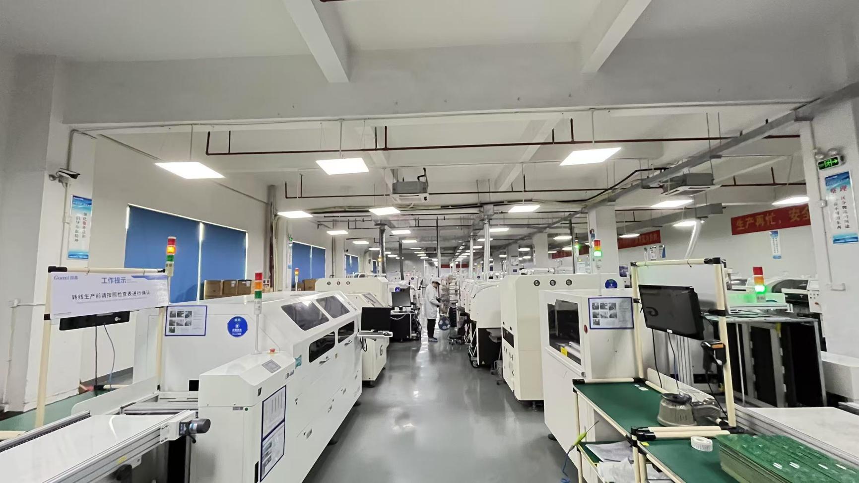
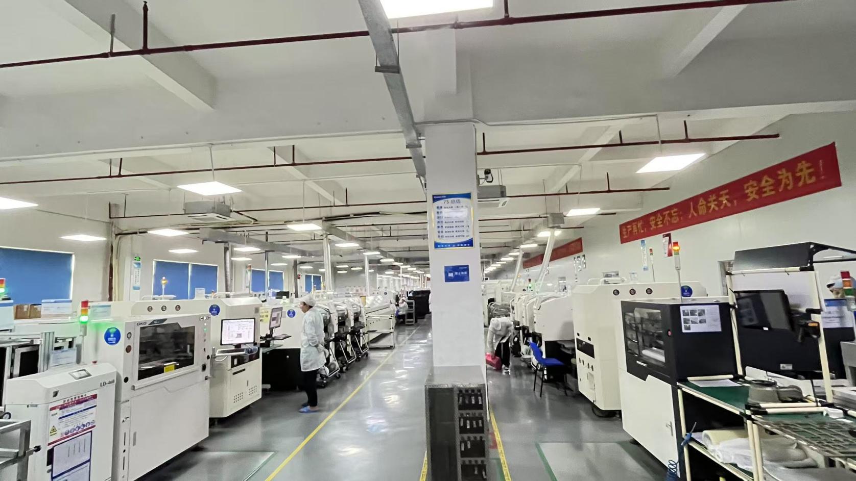
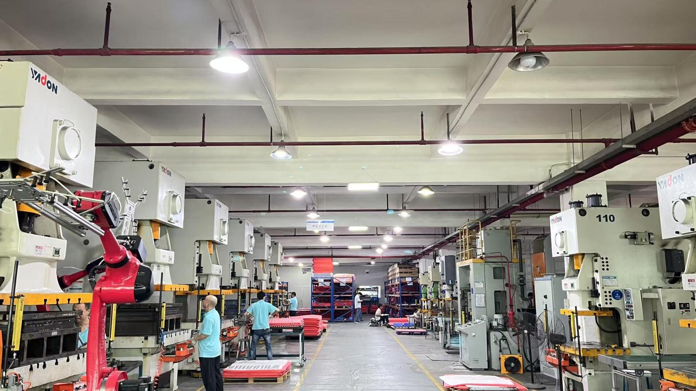
Strategically headquartered in China's high-tech manufacturing corridor, Vorynex Memory Technology (China) Co., Ltd. leverages a highly optimized supply chain that integrates high-frequency chip sourcing, precision copper-aluminum composite metal machining, and heavy-ounce PCB fabrication. While many global sourcing partners struggle with rising component costs, our local partnerships with over 1,200 raw material and DRAM silicon vendors secure a resilient supply line.
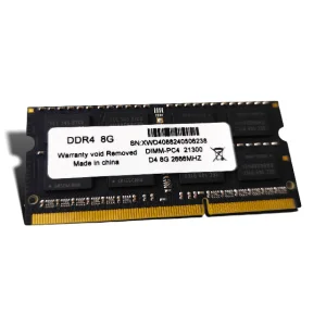
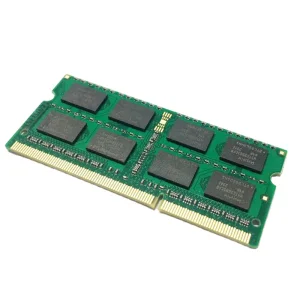
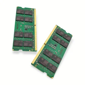
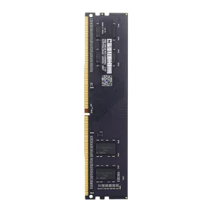
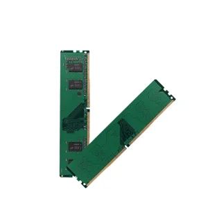
Heavy copper manufacturing is not just about layering metal; it demands precise chemical control and micro-etching to ensure vertical trace walls. Our manufacturing ecosystem excels in this. By deploying state-of-the-art multi-layer laminators and heavy-current electroplating baths, we guarantee uniformity in multi-layer structures, allowing delicate signal lines (like those required for DDR4 and DDR5 memory modules) to run adjacent to high-power distribution lines on the same substrate.
This operational excellence enables Vorynex to control manufacturing costs while offering extensive customization, including frequency tuning, customized PCB design, thermal heatsink optimization, and dedicated firmware tuning for global industrial and B2B buyers.
Consistency is guaranteed by our 100% testing standard. Every board undergoes strict Automated Optical Inspection (AOI), In-Circuit Testing (ICT), high-temperature thermal cycle stress testing, and final system-level validation. This rigorous QC process eliminates early failures and ensures field reliability.

Where precision meets high current: mapping heavy copper circuit board configurations to leading technological frontiers.
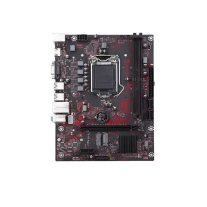
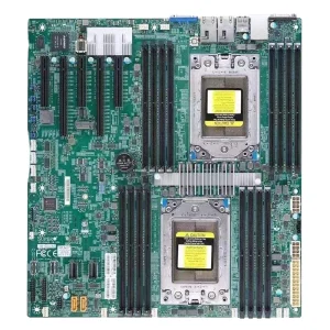
High-performance computing, particularly AI data centers and dual-socket server motherboards, demands massive currents at low voltages. High-power motherboards and power-distribution backplanes utilize heavy copper designs to feed multi-phase VRMs, ensuring low ripple, high efficiency, and minimal voltage drop under sudden load swings.
Electric vehicles utilize thick copper boards for main inverter modules, battery management systems (BMS), and fast-charging converters. The ability of thick copper to handle high currents and withstand constant engine bay vibration makes it a preferred choice for automotive reliability standards (AEC-Q100).
Heavy industrial motor controls, solar converters, and grid-tied systems rely on thick copper boards to manage heavy electrical loads. By optimizing the thermal path through composite copper-aluminum backing plates, system operating temperatures drop significantly, extending the lifespan of onboard power components.
Understand the performance trade-offs and trace geometry design limits of different copper weights.
| Parameters | Standard Copper PCB | Heavy Copper PCB | Extreme Copper PCB |
|---|---|---|---|
| Typical Copper Weight | 0.5 oz - 2 oz (17.5µm - 70µm) | 3 oz - 8 oz (105µm - 280µm) | 10 oz - 20+ oz (350µm - 700+µm) |
| Current Carrying Capacity | Low (< 15 Amperes) | Medium-High (15 - 100 Amperes) | Very High (100 - 300+ Amperes) |
| Min Trace Width / Spacing | 3 mils / 3 mils (0.075mm) | 8 mils / 10 mils (0.2mm - 0.25mm) | 15 mils / 20 mils (0.38mm - 0.5mm) |
| Thermal Performance | Requires external heatsinks | Self-cooling copper surface paths | Direct thermal path metal bonding |
| Common Applications | Mobile devices, consumer electronics | Servers, motor controls, EV BMS | Welding devices, solar switchgear, transformers |
Technical insights and engineering advice on integrating heavy copper boards into your system architecture.