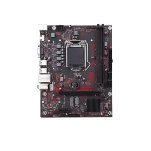
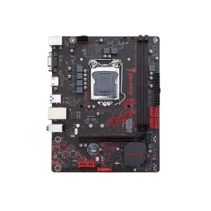
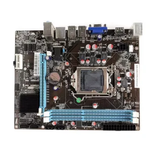
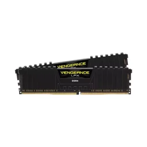
Select premium, high-frequency multilayer substrates, industrial memory chip assemblies, and server motherboards optimized for mission-critical enterprise architectures.
Decoding macroeconomic shifts, signal integrity requirements, and high-frequency trace routing trends across key high-tech corridors.
In modern industrial and commercial computing, the demand for Multilayer Printed Circuit Boards (PCBs) has reached unprecedented heights. Driven by high-performance computing (HPC), artificial intelligence server clusters, advanced telecom networks (5G/6G), and miniature medical devices, the global multilayer PCB industry is witnessing a structural transformation. In high-speed data transmission, legacy double-sided boards fail to meet the signal integrity, power distribution network (PDN), and thermal management requirements of modern high-frequency circuits. High-Density Interconnect (HDI) technology, combined with complex multilayer structures (commonly extending beyond 8 to 32 layers for high-tier server modules and memory controllers), has become the industry standard.
Geographically, manufacturing and supply chain hubs have concentrated in East Asia, with China, Taiwan, Japan, and South Korea managing substantial production infrastructure. Meanwhile, design specifications are globally decentralized. Enterprise architectures in North America and Western Europe require stringent compliance, such as UL94V-0, IPC-Class 3, and strict ITAR rules. To balance cost-efficiency with uncompromising signal fidelity, companies source components from certified partners capable of running sub-3 mil trace/space tolerances on complex stackups with high-performance copper foils and low-loss dielectrics like Megtron 6 and Rogers.
A deep dive into layer stackups, impedance control, dielectric materials, and production standards.
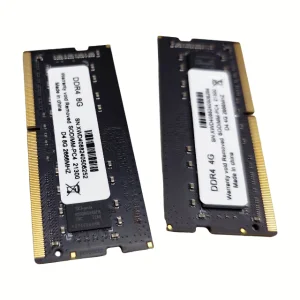
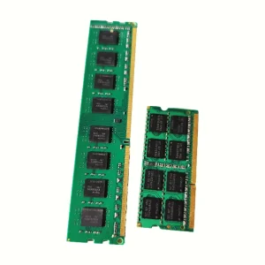
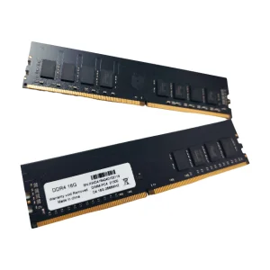
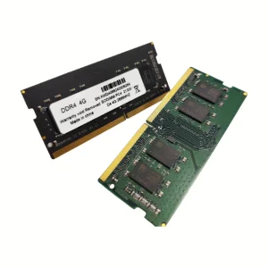
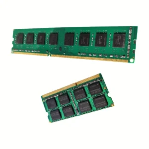
Modern multilayer boards rely on blind vias, buried vias, and microvias via sequential lamination. This allows routing across dense areas like 0.8mm and 0.5mm pitch BGAs found in modern DDR5 RAM and FPGA packages, maximizing board efficiency while minimizing crosstalk.
To avoid delamination during reflow or operations, high-Tg (glass transition temperature) FR4, Megtron, and ceramic-filled Rogers dielectrics are chosen. These materials minimize dielectric loss (Df) and dielectric constant (Dk), vital for multi-gigabit data paths.
By defining uniform reference ground planes adjacent to signal layers, RF and high-speed data transmission lines are matched to 50Ω single-ended and 90/100Ω differential configurations, crucial for high-speed DDR4/DDR5 system integrity.
A rigorous engineering evaluation of the substrate materials utilized in modern high-speed high-layer count designs. Selecting the right dielectric is the foundation of high-frequency signal design.
| Material Family | Typical Dielectric Constant (Dk) | Dissipation Factor (Df) | Glass Transition (Tg) | Primary Application Fields |
|---|---|---|---|---|
| Standard High-Tg FR-4 | 4.2 - 4.6 | 0.015 - 0.020 | 170°C - 180°C | Standard industrial computing, general electronics, consumer motherboards |
| Mid-Loss / High-Speed (e.g., Nelco) | 3.6 - 3.9 | 0.008 - 0.012 | 180°C - 200°C | Premium servers, enterprise networking switches, DDR4 high-speed memory cards |
| Ultra-Low-Loss (e.g., Megtron 6) | 3.4 - 3.7 | 0.002 - 0.004 | 185°C - 210°C | High-end DDR5 circuits, artificial intelligence accelerators, backplanes |
| PTFE/Ceramic (e.g., Rogers 4350B) | 3.48 ± 0.05 | 0.0037 | > 280°C | Radar assemblies, aerospace telecommunications, microwave antennas |
A professional evaluation matrix to assess capabilities, engineering expertise, and quality control systems.
Evaluating potential multilayer PCB suppliers requires looking beyond simple per-unit costs. Quality failures at high-layer counts can lead to expensive recalls, signal faults, and component damage. Global procurement teams use a structured framework based on these criteria:
A premier global manufacturer bridging advanced multilayer PCB fabrication with world-class memory module packaging and engineering.
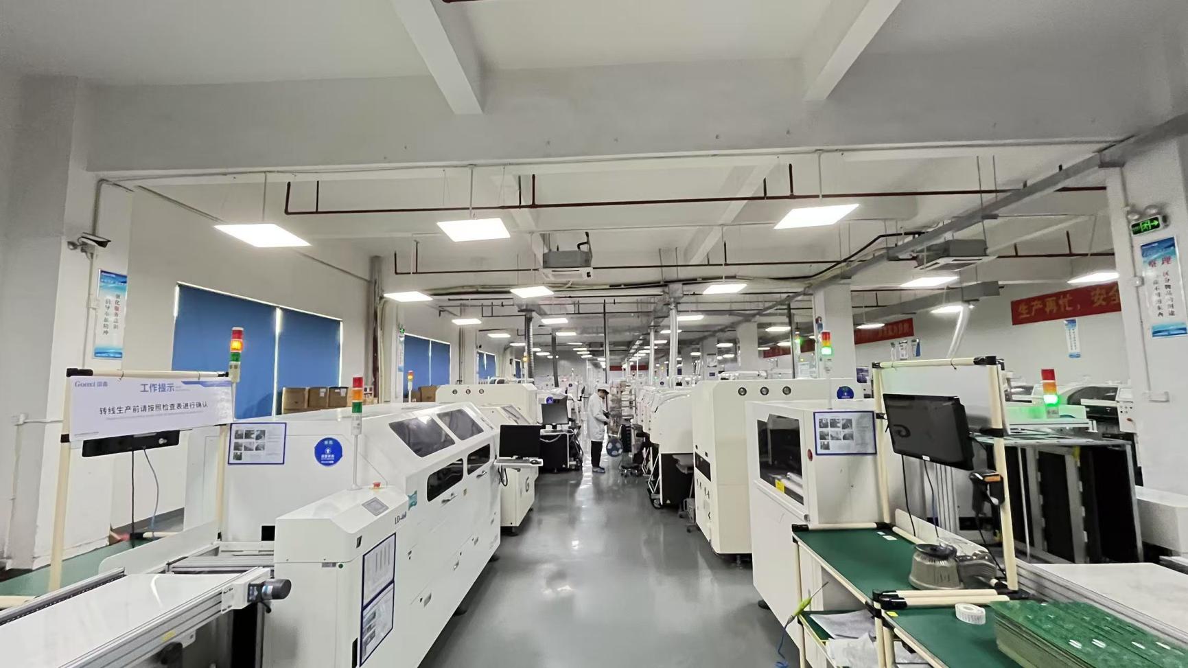
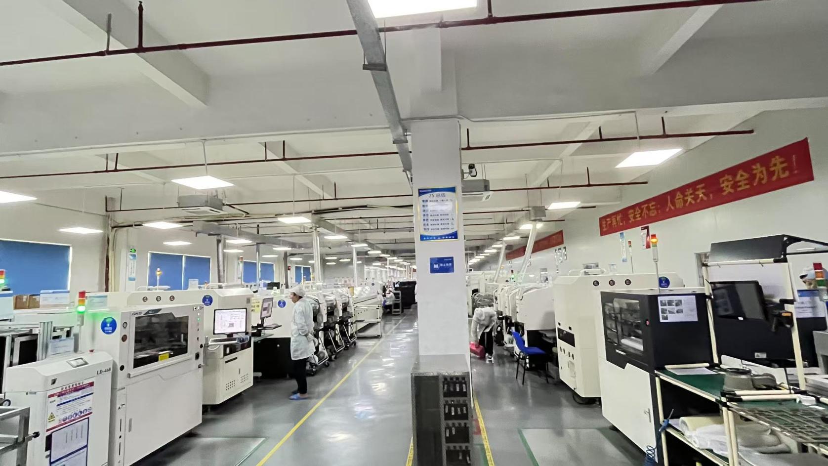
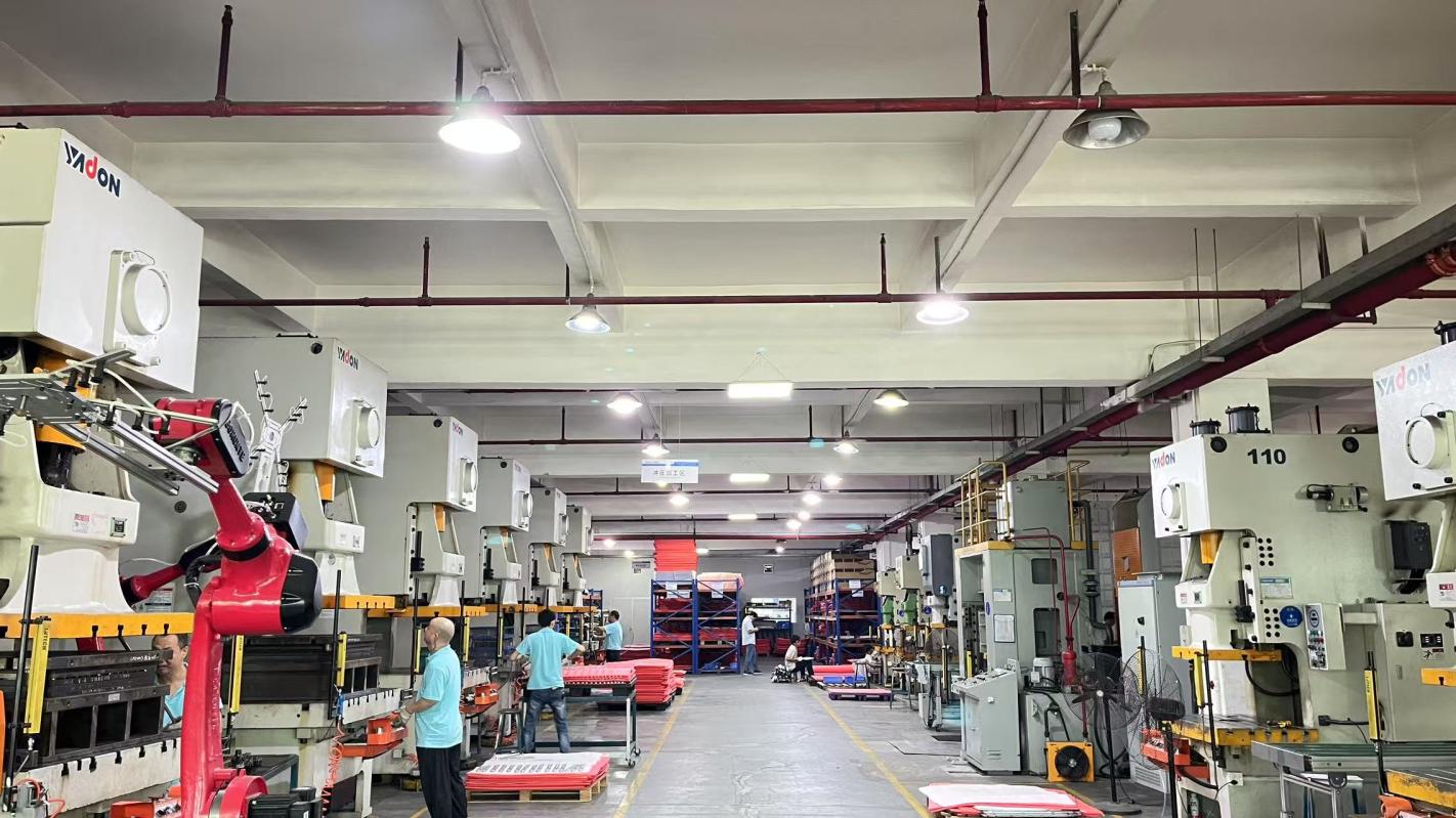
Established in 2016, Vorynex Memory Technology (China) Co., Ltd. has developed strong manufacturing and engineering capabilities over the years. With a modern production facility covering approximately 320㎡, Vorynex focuses on delivering stable, high-speed, and energy-efficient memory solutions for gaming, industrial, and enterprise applications.
The company achieved an annual export revenue of approximately USD 12 million, supported by 6 years of export experience and over 12 years of industry experience in memory and semiconductor-related fields. Through continuous R&D and engineering refinement, Vorynex bridges the gap between raw PCB fabrication and system-level electronic performance.
With a strong international trade background, Vorynex serves key markets including North America, Europe, Southeast Asia, the Middle East, and South America. The company collaborates with more than 1,200 supply chain partners, enabling stable sourcing of high-quality DRAM chips and components. Its primary customer base includes brand distributors, system integrators, industrial equipment manufacturers, and gaming hardware companies. Supported by a team of approximately 180 R&D engineers, the company focuses on memory architecture optimization, compatibility enhancement, and thermal performance improvement.
Customization is fully supported, including frequency tuning, PCB design customization, heat sink design, branding (private label), and firmware optimization. In the past year, the company successfully launched around 240 new product models, covering DDR4, DDR5, and specialized industrial memory solutions.

How multilayer PCBs and system-level packages function in demanding localized environments.
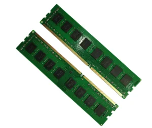
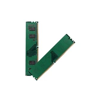
Servers processing petabytes of data rely on motherboards built with 16 to 32 layers of ultra-low-loss material. High-frequency routing requires matching length variations down to mils to prevent timing skew across multi-channel memory busses like DDR4/DDR5.
Factory-floor controllers run in noisy, hot environments. Heavy copper multilayer PCBs and aluminum substrates protect low-voltage control signals from electromagnetic interference (EMI) and help dissipate excess heat.
5G/6G base station transceivers operate at high frequencies. They utilize hybrid multilayer boards, bonding standard FR-4 layers for structural routing with high-frequency Rogers laminates on the outer RF layers.
Key design developments and production methodologies shaping the next decade of electronic hardware.
As computing requirements push physical limits, conventional PCB fabrication must adapt. These key technologies are defining the roadmap for multilayer board fabrication:
Technical answers to key engineering and procurement questions to help you mitigate project risk.
Browse our selection of performance memory modules, gaming RAM, and server motherboard solutions.