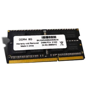
The global storage and memory ecosystem is undergoing an unprecedented architectural shift. As artificial intelligence (AI), edge computing, 5G infrastructures, and cloud databases expand exponentially, the demand for high-throughput, low-latency storage systems has escalated. Solid State Drives (SSDs) and dynamic memory modules serve as the silicon-based nervous system of this transformation. China, as the world's primary manufacturing hub for electronic systems, has transitioned from a mere assembly line region to a pioneer in storage controller design, firmware innovation, and rigorous quality control workflows.
Understanding the distinction between consumer-grade client drives and enterprise-grade storage structures is crucial for procurement officers, system integrators, and industrial designers. While consumer drives optimize burst performance and pricing, enterprise storage solutions demand high Terabytes Written (TBW) metrics, predictable IOPS consistency, Power Loss Protection (PLP), and advanced hardware-level ECC (Error Correction Code) subsystems. Navigating this dense technological ecosystem requires deep alignment with a manufacturing partner capable of end-to-end customization, comprehensive quality validation, and robust supply chain integration.
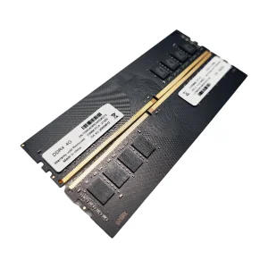
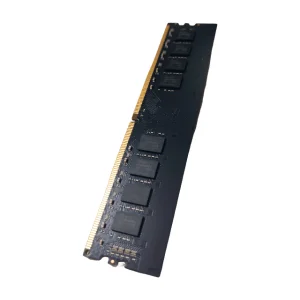
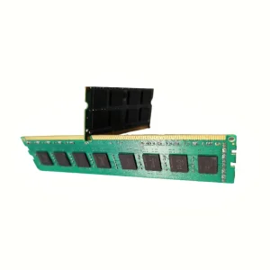
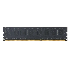
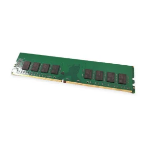
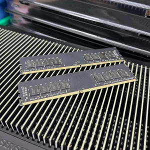
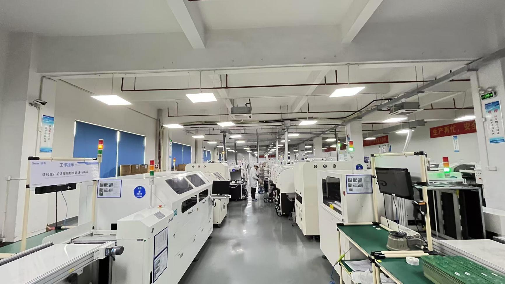
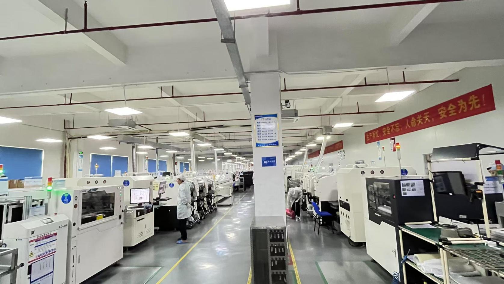
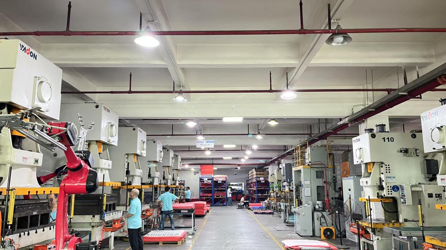
Established in 2016, Vorynex Memory Technology (China) Co., Ltd. has positioned itself at the vanguard of the memory and solid-state storage industry. As a professional DDR5 memory manufacturer and OEM/ODM solution provider, the company specializes in engineering high-performance memory modules tailored to the stringent demands of international markets. Our state-of-the-art production facility spanning approximately 320㎡ delivers highly optimized, stable, high-speed, and energy-efficient memory architectures designed for gaming, industrial control systems, and enterprise data server arrays.
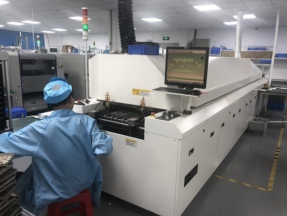
Underpinning the reputation of Vorynex is a zero-defect manufacturing philosophy. Our structured quality control infrastructure comprises over 45 professional QC specialists who implement complex inspection methodologies at every phase of production. We do not compromise on reliability:
To future-proof global procurement pipelines, Vorynex aligns closely with memory layer innovations and controller hardware developments. Storage hardware engineering is evolving rapidly across three distinct paradigms:
Transitioning from 128-layer architectures toward 232-layer and 300+ layer designs. Multi-level cell architectures (TLC and QLC) are coupled with dynamic algorithms to offer higher capacities per square millimeter of silicon while mitigating structural wear.
Migration from SATA III (6 Gbps limit) to PCIe Gen 4 & Gen 5 NVMe interfaces. High-bandwidth pipelines operating on x4 lanes reach read/write speeds exceeding 14,000 MB/s, supported by LPDDR4/LPDDR5 DRAM cache design configurations.
Integrating on-die Power Management ICs (PMICs) and Hardware ECC on-chip. Moving operational frequencies past 4800MHz to 6400MHz and beyond, facilitating higher system efficiency and drastically reducing electrical consumption.
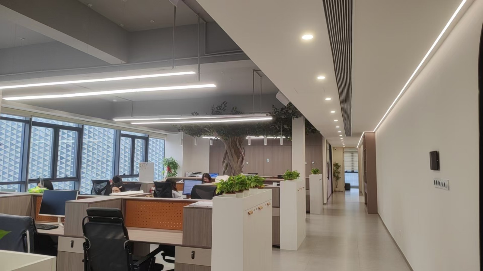
Vorynex's R&D team of 180 engineers manages memory architecture optimization, signal integrity simulation, thermal profile mapping, and Custom ASIC firmware engineering. In the past financial year, the R&D division successfully rolled out 240 new product configurations, reinforcing the company's positioning as an industry leader.
High-density SSDs configured with Power Loss Protection (PLP) capacitors, supporting mixed-use write endurance models (1 to 3 DWPD). Perfect for virtualization matrices, SQL databases, and real-time transaction processing networks.
Wide-temperature storage systems designed to operate under harsh thermal environments (-40°C to 85°C). Utilizing specialized conformal coatings to protect internal boards against moisture, particulate dust, and mechanical vibration.
Global client system integrators take advantage of Vorynex's comprehensive customization programs. This includes private branding label services, custom-designed aluminum heat spreader units, tailored firmware configs, and frequency optimizations.
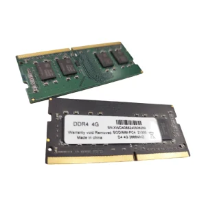
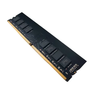
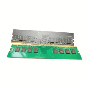
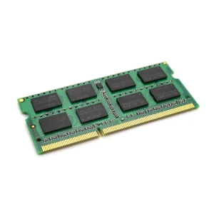
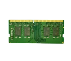

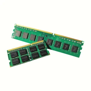
Developing bespoke memory and storage hardware demands a systematic approach. Our engineers work hand-in-hand with procurement departments to define specifications, mitigate design risks, and accelerate product time-to-market:
Our design capabilities extend beyond standard modules. We offer comprehensive frequency tuning, specialized PCB multi-layer routing configuration, aluminum heat spreader geometric design (including RGB integration and custom materials), and firmware modifications to adapt power tables and latency states for specific systems.
Leveraging over 1,200 secure supply chain partnerships, Vorynex provides a reliable supply of premium DRAM dies (Samsung, Micron, SK Hynix) and controller chipsets. This helps mitigate international trade instability and components pricing volatility.
For brand distributors and international system integrators, Vorynex offers end-to-end private labeling services. Our services cover box design, customized hardware laser etching, tailored user manuals, regulatory certification handling (FCC, CE, RoHS, UKCA), and drop-shipping options to secure global destinations.
 Vorynex