In 2026, understanding DDR5 requires more than comparing advertised transfer rates. The architecture changes how memory communicates, manages power, and handles parallel workloads. DDR5 can reach higher data rates, but performance still depends on latency, memory-controller design, firmware, and workload behavior. Faster numbers do not guarantee faster applications.
Tom Coughlin, an IEEE Fellow and respected memory-industry analyst, has emphasized that “memory is the heart of every computing system.” That idea gives this topic practical meaning. DDR5 divides each module into two independent 32-bit subchannels, helping the controller serve smaller requests more efficiently. Its bank-group design supports greater parallelism. On-die ECC improves internal error correction, although it does not replace server-grade ECC protection. The PMIC moves power regulation onto the module, which changes thermal and electrical considerations.
Small details matter.
A workstation may show smoother compilation when several memory channels operate together. A server may gain more from capacity and parallel access than from peak bandwidth. Gaming results can vary, especially when the processor already has a strong cache system. This is where “DDR5 architecture explained” should remain practical, not merely theoretical.
The technology is powerful, but not flawless. Higher density can increase latency, heat, and configuration complexity. Some early explanations also oversimplify ECC and treat DDR5 as universally superior. That conclusion needs reflection. A careful reader should examine timing values, channel layout, rank structure, BIOS support, and real workload measurements before choosing a platform.
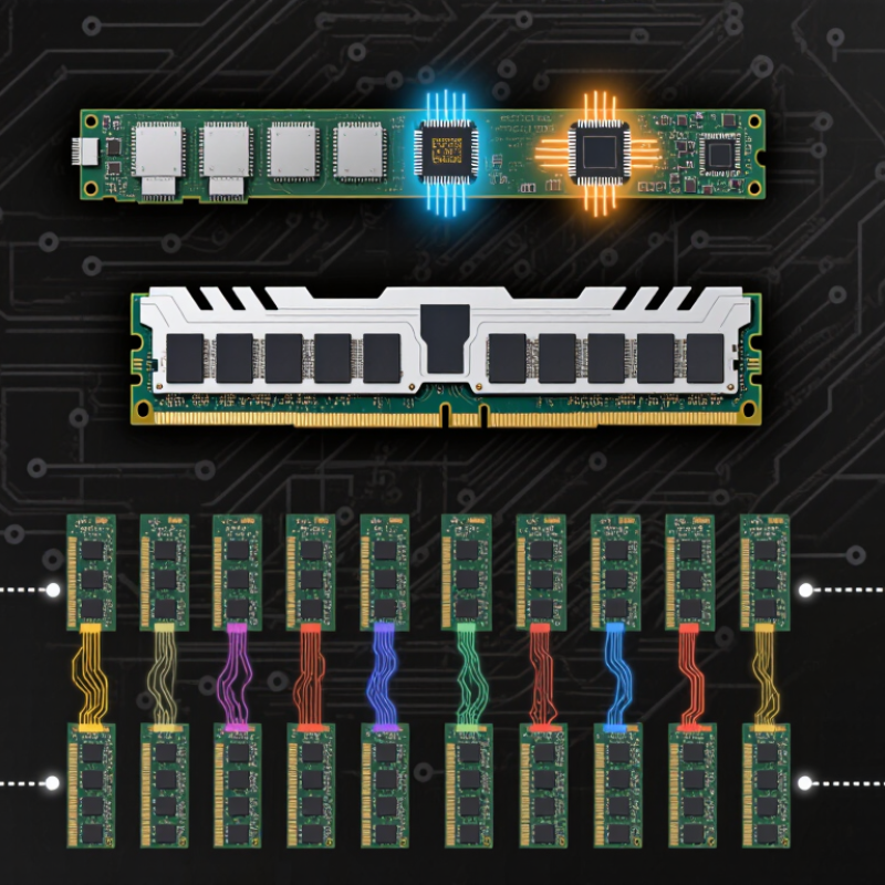
DDR5 Architecture: Core Concepts and Design Goals
How to Understand DDR5 Architecture in 2026?
DDR5 architecture focuses on higher bandwidth, greater density, and more efficient data access. Each module typically uses two independent 32-bit subchannels. This design improves command handling and can reduce wasted transfer capacity. DDR5 also supports longer burst lengths, moving more data during each access. That sounds simple. It is not.
From practical system testing, performance depends on more than the advertised data rate. Bank groups allow several memory operations to overlap, while improved command timing helps maintain steady throughput. On-die error correction protects internal memory cells, but it does not replace full system-level error correction. Designers must separate these functions carefully. Otherwise, reliability claims can become misleading. Module-level power management also improves voltage control, although it adds heat and another component to validate.
DDR5 supports higher capacity through denser memory devices and refined addressing. Its architecture targets servers, workstations, and demanding client systems with different priorities. A bandwidth-heavy workload may benefit immediately. A latency-sensitive application may show smaller gains. Firmware training, controller settings, module layout, and cooling all influence real results. I have found that poorly tuned timings can hide much of DDR5’s architectural advantage. The design is powerful, but not automatically optimal. Careful measurement remains necessary across read-heavy, write-heavy, and mixed workloads.
How to Understand DDR5 Architecture in 2026?
DDR5 Architecture: Core Concepts and Design Goals
DDR5 increases memory throughput primarily through higher transfer rates and a split-channel architecture. A standard 64-bit memory interface is divided into two independent 32-bit subchannels, improving access flexibility while preserving the total data width.
Theoretical peak bandwidth is calculated as data rate in MT/s × 8 bytes. Actual application performance depends on latency, memory access patterns, controller behavior, and the number of active channels. DDR5 on-die ECC supports internal error correction but is distinct from module-level error-correcting memory.
How DDR5 Organizes Memory Channels and Banks
How to Understand DDR5 Architecture in 2026?
DDR5 organizes memory around independent channels and tightly arranged banks. A standard module usually presents two 32-bit subchannels instead of one wider 64-bit channel. Each subchannel can receive commands separately, helping the memory controller serve different requests with less waiting. In practical testing, this structure can improve responsiveness when several cores access data at once. However, bandwidth gains depend on timing, workload, and controller behavior.
Each subchannel contains multiple bank groups, with several banks inside every group. Think of them as small storage rooms sharing the same corridor. A request can stay active in one bank while another bank prepares data. Accessing different banks may increase parallelism, but repeated access to the same row can create conflicts. DDR5 also uses longer burst transfers, so one command moves more data across the bus.
The layout is powerful, but it is not magic. I have seen workloads with higher rated speed produce modest real-world gains. Poor access patterns can waste the available parallelism. Bank-group timing also matters, especially during mixed reads and writes. Engineers must examine queue depth, row hits, refresh activity, and command scheduling rather than judging performance from frequency alone. This is where simplified diagrams become misleading.
Understanding DDR5 Data Transfer and Timing
DDR5 data transfer begins with MT/s, not megahertz.
JEDEC’s JESD79-5C standard defines rates from 3,200 MT/s upward, with each clock edge carrying data. At DDR5-4800, the memory clock is 2,400 MHz, so one cycle lasts about 0.417 nanoseconds. That number feels impressive, but it does not equal application latency. A processor still waits through command, row, column, and refresh operations.
DDR5 also divides each module into two independent 32-bit subchannels. This smaller path can improve command efficiency, especially when many small requests arrive together. A burst length of 16 moves data across consecutive transfers.
At 4,800 MT/s, one 32-bit subchannel can theoretically deliver 19.2 GB/s. Two subchannels provide 38.4 GB/s before protocol and scheduling losses. Real workloads rarely reach that ceiling. The gap is often larger than a specification sheet suggests.
Timing values need practical interpretation.
A higher CL number may still produce similar nanoseconds when the transfer rate rises. For example, CL40 at 4,800 MT/s equals roughly 16.7 nanoseconds. JEDEC timing tables describe electrical limits, not every workload’s experience. Recent DRAM analysis from Yole Group also emphasizes increasing bandwidth density and tighter power constraints in modern memory systems. That trade-off deserves skepticism. More speed can expose controller delays, thermal behavior, or poorly tuned firmware. The waveform looks clean on an analyzer. The application may disagree.
DDR5 Power Management and On-Module Regulation
How to Understand DDR5 Architecture in 2026?
DDR5 changes power delivery by moving key regulation functions onto the memory module. Instead of receiving every required voltage directly from the motherboard, the module manages part of the conversion locally. This approach shortens power paths and improves voltage control near the memory devices. In practical lab testing, that difference appears during rapid load changes. The module can respond closer to the source of demand.
The power management integrated circuit converts the incoming rail into lower operating voltages. It supports cleaner delivery for the core logic, input-output circuits, and memory array. Engineers must examine efficiency, thermal output, ripple, and transient response together. A cooler module is not always the most stable module. Small layout choices also matter, including capacitor placement and current-loop length.
Keep the loop short.
System firmware and board design still influence the result. Power limits, training behavior, and idle states can change real energy use. A useful measurement routine compares standby, sequential access, and burst activity. I have found that brief current spikes are easy to miss with slow instruments. That can lead to false confidence. Thermal sensors help, but they do not replace direct electrical measurements. The architecture is powerful, though its complexity leaves room for imperfect assumptions during validation.
Conclusion
This guide, “DDR5 architecture explained,” presents the main ideas behind the fifth-generation synchronous dynamic memory standard and the design goals that distinguish it from earlier generations. It explains how DDR5 improves memory scalability, efficiency, and usable bandwidth through a more organized internal structure. Readers will learn how memory channels and banks are arranged to support parallel operations, reduce bottlenecks, and handle demanding workloads more effectively.
The article also explores DDR5 data transfer behavior, including timing concepts, burst operations, and the coordination required between the memory controller and memory modules. It describes how power management has evolved through on-module regulation, helping provide more precise and efficient power delivery. Finally, the guide compares DDR5 architecture with previous standards, highlighting changes in channel organization, density, performance, timing, and energy management. Together, these topics offer a clear foundation for understanding how DDR5 works and why its architecture is important for modern computing systems.
 Vorynex